Effect of concentration on the crystallographic and FTIR properties of lead sulphide (PbS) thin films
Keywords:
PbS thin film, SILAR cycle, NanocrystallinityAbstract
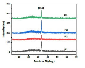
This study reports the use of the successive ionic layer adsorption and reaction (SILAR) technique as a low-cost and rapid method for depositing lead sulphide (PbS) thin films. The films were deposited on soda-lime glass (SLG) substrates by varying the molar concentrations of lead ions (0.3, 0.5, and 0.7 M) at a constant SILAR cycle number of 25. X-ray diffraction (XRD) patterns showed that the deposited PbS thin films were crystalline and had a cubic structure. Fourier-transform infrared (FTIR) spectroscopy indicated nanocrystalline PbS thin films with weak-to-medium M--O bonding. The O--H stretching vibration appeared at 3419.10 cm-1. Bands at 1338.90 and 1220.10 cm-1 were associated with improved crystallinity and C--O stretching vibrations. N--H group vibrations were observed at 1686.42 and 1597.87 cm-1, whereas CH2 bending vibrations occurred between 1482.79 and 1441.44 cm-1.
References
[1] O. O. Abegunde, E. T. Akinlabi, O. P. Oladijo, S. Akinlabi & A. U. Ude, ``Overview of thin film deposition techniques'', AIMS Materials Science 6 (2019) 174. https://doi.org/10.3934/matersci.2019.2.174.
[2] C. E. Pérez-García, S. Meraz-Dávila, G. Arreola-Jardón, F. de Moure-Flores, R. Ramírez-Bon & Y. V. Vorobiev, ``Characterization of PbS films deposited by successive ionic layer adsorption and reaction (SILAR) for CdS/PbS solar cells application'', Materials Research Express 7 (2020) 015530. https://doi.org/10.1088/2053-1591/ab6b5c.
[3] E. Yücel, Y. Yücel & B. Beleli, ``Process optimization of deposition conditions of PbS thin films grown by a successive ionic layer adsorption and reaction (SILAR) method using response surface methodology'', Journal of Crystal Growth 422 (2015) 1. https://doi.org/10.1016/j.jcrysgro.2015.04.018.
[4] M. Stoian, T. Maurer, S. Lamri & I. Fechete, ``Techniques of preparation of thin films: Catalytic combustion'', Catalysts 11 (2021) 1530. https://doi.org/10.3390/catal11121530.
[5] F. Göde, F. Yavuz & I. A. Kariper, ``Preparation and characterization of nanocrystalline PbS thin films produced by chemical bath deposition'', Acta Physica Polonica A 128 (2015) B-215. https://doi.org/10.12693/APhysPolA.128.B-215.
[6] A. S. Obaid, M. A. Mahdi, A. Ramizy & Z. Hassan, ``Structural properties of nanocrystalline PbS thin films prepared by chemical bath deposition method'', Advanced Materials Research 364 (2012) 60. https://doi.org/10.4028/www.scientific.net/AMR.364.60.
[7] H. M. Pathan & C. D. Lokhande, ``Deposition of metal chalcogenide thin films by successive ionic layer adsorption and reaction (SILAR) method'', Bulletin of Materials Science 27 (2004) 85. https://doi.org/10.1007/BF02708491.
[8] S. Rajathi, K. Kirubavathi & K. Selvaraju, ``Structural, morphological, optical, and photoluminescence properties of nanocrystalline PbS thin films grown by chemical bath deposition'', Arabian Journal of Chemistry 10 (2017) 1167. https://doi.org/10.1016/j.arabjc.2014.11.057.
[9] F. Solis-Pomar, A. Fundora Cruz, J. L. Menchaca, M. F. Meléndrez & E. Pérez-Tijerina, ``Study of the structural properties of nanostructured PbS thin films deposited by RF sputtering at room temperature'', Materials Research Express 5 (2018) 106403. https://doi.org/10.1088/2053-1591/aadac0.
Published
How to Cite
Issue
Section
Copyright (c) 2026 Qasim A. Adeniji, Taiwo O. Roy-Layinde, Dasola B. Adeniji, Temitope O. Fowodu, Ayobamidele D. Adelaja, Abdulganiu D. Adeniji, Muhammad A. Salihu, Oludele Adegboyega, Kola Odunaike (Author)

This work is licensed under a Creative Commons Attribution 4.0 International License.